How AI Deployment in Electronics Manufacturing Actually Works on the Line
Walk into any contract electronics manufacturing facility today and you'll hear the same questions echoing from the NPI team to the SMT floor: where does AI actually fit, and how do we make it work without disrupting production? The reality of AI deployment in electronics manufacturing isn't what the vendor brochures show. It's not a single software install or a plug-and-play vision system. It's a methodical integration across multiple touchpoints—from component kitting to reflow profiling to test data analysis—where the technology has to prove itself against the unforgiving metrics of first pass yield and cycle time.
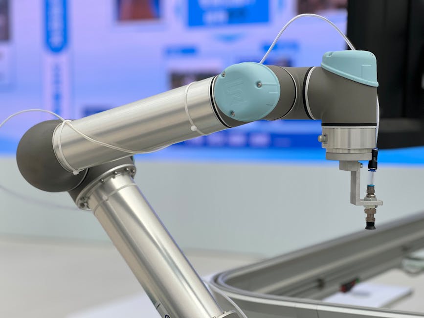
Understanding AI Deployment in Electronics Manufacturing requires looking past the hype and seeing what actually happens when machine learning models meet the reality of SMT line constraints, BOM variability, and the daily pressure of customer delivery commitments. The deployment path splits into three distinct operational layers, each with its own technical requirements and integration challenges. Let's examine how AI moves from pilot to production in a working EMS environment.
Layer One: Component and Material Intelligence
The first integration point sits upstream of the SMT line itself, in the material staging and kitting area. This is where AI deployment in electronics manufacturing begins to touch BOM scrubbing, supplier data reconciliation, and AVL validation. Traditional ERP systems handle the transactional logic—part numbers, quantities, lead times—but they can't predict which supplier lots are statistically more likely to cause placement issues or reflow defects based on historical patterns across multiple builds.
AI models trained on component-level failure data can flag high-risk material before it reaches the feeder bank. The system ingests inspection reports from incoming quality control, correlates them with SMT defect logs from prior runs, and scores each lot. When a new reel of 0402 capacitors arrives from an alternate supplier on the AVL, the model compares its moisture sensitivity level, packaging type, and supplier quality history against past placements. If the risk score crosses a threshold, the material planner receives an alert before the kitting process begins.
This deployment doesn't require replacing existing MES or ERP infrastructure. Instead, the AI layer operates as middleware, pulling data from inspection databases and feeding recommendations back into work order planning. The technical challenge is data standardization—ICT failure codes, AOI defect classifications, and X-ray inspection results all use different schemas. Deployment teams spend weeks mapping these taxonomies before the first model trains. But once operational, this layer reduces first article inspection failures by surfacing material risks that human BOM scrubbers would miss in the compressed timelines of NPI ramp.
Layer Two: Process Control and Real-Time Adjustment
The second layer integrates directly with SMT equipment—pick-and-place machines, solder paste printers, reflow ovens. Here, AI deployment in electronics manufacturing shifts from prediction to active process control. Modern placement equipment already generates massive telemetry: nozzle vacuum pressure, vision system confidence scores, placement force, feeder advance timing. Reflow ovens log zone temperatures and conveyor speed every few seconds. Traditional SPC tracks these parameters within control limits, but AI models can detect multivariate drift patterns that single-variable Cp/Cpk calculations miss.
A practical example: during a high-mix production day with frequent changeovers, the stencil printer runs different aperture designs and solder paste types across multiple boards. An AI model monitoring solder paste inspection (SPI) data recognizes that a specific combination—particular paste viscosity, ambient humidity level, and squeegee pressure—is trending toward the lower acceptance boundary for paste volume. Instead of waiting for an SPI rejection to halt the line, the system alerts the SMT operator and suggests a squeegee pressure adjustment. The operator validates the recommendation, makes the change, and the line continues without a stoppage.
Integration with Existing Equipment Control Systems
Deploying this capability requires APIs or OPC UA connections into equipment controllers. Not all SMT platforms expose the necessary data streams, and older legacy lines may need edge computing hardware to bridge the gap. The deployment often starts with one pilot line—typically the newest equipment set with the best data access—before expanding to older generations. Many operations utilize generative AI integration services to build custom connectors when equipment vendors don't provide standardized interfaces.
The ROI calculation for this layer focuses on OEE improvement and reduction in unplanned line stoppages. In high-volume runs, even a five-minute reduction in average time between SPI failures translates to measurable throughput gains. For low-volume, high-mix NPI work, the benefit shifts to faster debug cycles when new boards enter production. AI for SMT Operations at this level doesn't eliminate the need for skilled operators and process engineers—it extends their situational awareness across more variables than they can monitor simultaneously on a manual basis.
Layer Three: Test, Yield Analysis, and Defect Attribution
The third deployment layer sits downstream at in-circuit test (ICT), functional test (FCT), and final inspection. This is where AI deployment in electronics manufacturing addresses the hardest question in yield management: why did this board fail, and which upstream process caused it? Traditional test systems report pass/fail and log fault signatures, but attributing a test failure back to a specific SMT defect, a component quality issue, or a design weakness requires forensic analysis that happens manually during CAPA investigations.
AI models trained on correlated datasets—test failure logs, AOI defect images, X-ray inspection results, and rework records—can perform automated root cause clustering. When an ICT station flags a short on a power rail, the AI system retrieves the board's process history: which SMT line placed the components, what the reflow profile looked like, whether AOI flagged any anomalies that were accepted as false calls, and if similar failures appeared on other boards from the same panel. The model surfaces the most probable root cause and ranks contributing factors.
This capability accelerates First Pass Yield Optimization by shortening the feedback loop from test failure to process correction. In traditional workflows, a yield issue might take days to diagnose through failure analysis meetings and manual data correlation. With AI-driven defect attribution, the test engineering team identifies the likely cause within hours and routes corrective action to the right process owner—whether that's an SMT setup adjustment, a component quality issue requiring supplier notification, or an ECO to address a design-for-manufacturability gap.
Deployment Challenges in Test Data Integration
The technical barrier here is integrating siloed test systems that weren't designed to share data. ICT platforms, flying probe testers, boundary scan systems, and functional test rigs often come from different vendors with proprietary data formats. Deploying AI in this layer requires building a unified test data warehouse that normalizes failure signatures and links them to board serial numbers and process genealogy. Many EMS providers tackle this incrementally, starting with their highest-volume product lines where the statistical dataset is richest and the business case is strongest.
For AI in NPI, this layer becomes particularly valuable during production ramp. New product introductions compress the learning curve—first articles need to move through design validation, process qualification, and production ramp in weeks rather than months. AI-driven defect attribution helps NPI teams identify DFM issues faster, prioritize which ECOs deliver the most yield impact, and validate process changes without waiting for statistically significant sample sizes from manual SPC tracking.
How These Layers Connect in Practice
In a fully deployed environment, all three layers communicate. A test failure attributed by Layer Three to a solder joint defect triggers a review of Layer Two's reflow telemetry for that specific board. If the data shows a minor temperature excursion that stayed within SPC limits but correlates with similar failures, the system flags it for process engineering review. Layer One checks whether the component supplier for the affected part number has a history of moisture sensitivity issues that might explain reflow behavior. The combined insight—supplier material variability plus marginal reflow profile—drives a corrective action that addresses both root causes.
This integrated approach is where AI deployment in electronics manufacturing delivers compounding value beyond point solutions. A standalone AOI system with AI-enhanced defect detection improves inspection accuracy, but it's still a single-point tool. When defect detection feeds into process control, which informs material risk scoring, which links back to test yield analysis, the system becomes a closed-loop intelligence layer across the entire value stream.
Deployment timelines for this integrated model typically span 12 to 18 months in a mid-sized EMS operation. The first six months focus on data infrastructure—building pipelines, cleaning historical datasets, standardizing taxonomies. Months six through twelve deploy Layer One and Layer Two pilots on selected product families. The final phase integrates Layer Three and establishes cross-layer workflows. Throughout this timeline, change management is as critical as technical integration. SMT operators, test engineers, and NPI program managers need training not just on using AI tools, but on interpreting model outputs and understanding when to override recommendations based on domain expertise the model doesn't capture.
Conclusion
The operational reality of AI deployment in electronics manufacturing is less about revolutionary transformation and more about methodical augmentation of existing processes. It doesn't replace BOM scrubbing, SPC, or failure analysis—it makes those activities faster and more precise by processing multidimensional data at scale. Success depends on data infrastructure, cross-functional collaboration, and a deployment roadmap that prioritizes high-impact integration points over comprehensive coverage. For EMS providers navigating this path, the key is starting with clear ROI targets—whether that's FPY improvement, NPI cycle time reduction, or DPPM reduction—and building the deployment plan backward from those measurable outcomes. Organizations looking for structured guidance can benefit from an AI Implementation Framework that maps technical capabilities to operational objectives and sequences deployment across the three layers in a logical progression.


Comments
Post a Comment